● 1N5333B thru 1N5388B 5W Silicon Zener Diode - Topdiode
1N5333B thru 1N5388B 5W Silicon Zener Diode are used to generate low power stabilized supply rails from a higher voltage and to provide reference voltages for circuits, especially stabilized power supplies.
● 1N5333B thru 1N5388B 5W Silicon Zener Diode - Topdiode Introduction
1N5333B thru 1N5388B 5W Silicon Zener Diode is in DO-201AE package with the type designation from 1N5333B thru 1N5388B. offer wide voltage from 3.3V to 200V.
● 1N5333B thru 1N5388B 5W Silicon Zener Diode Features
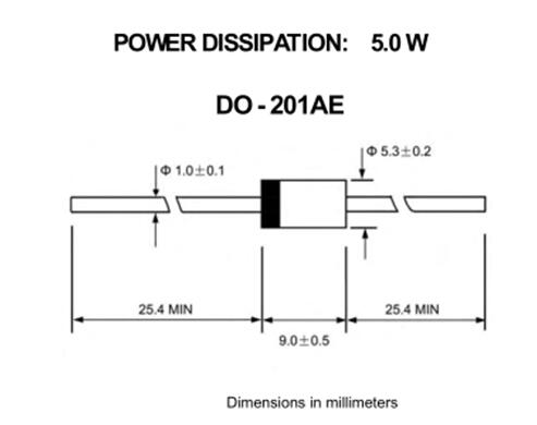
* Case: DO-201AE
* Total power dissipation: 5 W
* Standard tolerance +/-10% & suffix “B” for +/-5% tolerance and other zener voltage and tolerances are available on request
● 1N5333B thru 1N5388B 5W Silicon Zener Diode Applications
* Voltage stabilization
●
● 1N5333B thru 1N5388B 5W Silicon Zener Diode Outlines and External Dimensions
● 1N5333B thru 1N5388B 5W Silicon Zener Diode Qualification, Lead time, Shipping Terms
* RoHS Compliant
* REACH Compliant
* Ex-work, FCA , or FOB
* 4-6 weeks, regular stock available
● 1N5333B thru 1N5388B 5W Silicon Zener Diode Maximum Ratings
MAXIMUM RATINGS AND ELECTRICAL CHARACTERISTICS
Ratings at 25 ambient temperature unless otherwise specified.
Single phase,half wave,60 Hz,resistive or inductive load. For capacitive load,derate by 20%.
|
|
SYMBOL
|
VALUE
|
UNIT
|
|
Zener current (see Table "Characteristics")
|
|
|
|
|
DC pow er dissipation @ TL=75, measure at zero lead length (Fig.1) derate above 75 (NOTE 1)
|
PD
|
5.0
40.0
|
W
mW
|
|
Peak forw ard surge current 8.3ms single half sine-w ave superimposed on rated load (JEDEC Method)(NOTE 1,2)
|
IFSM
|
see fig.5
|
A
|
|
Junction temperature
|
TJ
|
-55---+150
|

|
|
Storage temperature range
|
Ts
|
-55---+150
|
|
NOTES: (1) Mounted on 8.0mm2 copper pads to each terminal.
(2) 8.3ms single half sine-wav e, or equiv alent square wav e, duty cycle=4 pulses per minute maximum.
● 1N5333B thru 1N5388B 5W Silicon Zener Diode Electrical Characteristics
1N5333B-1N5388B Zener Diodes
ELECTRICAL CHARACTERISTICS (TA=25℃)
|
Type (Note 1)
|
Zener voltage (Note 2)
|
Maximum Zener Impedance (Note 2)
|
Max Reverse Leakage Current
|
IR
(Note 3) A
|
VZ
(Note 4) V
|
IZM
(Note 5) mA
|
|
VZ@IZTV
|
IZT
mA
|
ZZT@IZT
Ω
|
ZZT@IZK=1mA
Ω
|
IR
|
VR
|
|
mA
|
V
|
|
1N5333B
|
3.3
|
380
|
3.0
|
400
|
300
|
1.0
|
20
|
0.85
|
1440
|
|
1N5334B
|
3.6
|
350
|
2.5
|
500
|
150
|
1.0
|
18.7
|
0.80
|
1320
|
|
1N5335B
|
3.9
|
320
|
2.0
|
500
|
50
|
1.0
|
17.6
|
0.54
|
1220
|
|
1N5336B
|
4.3
|
290
|
2.0
|
500
|
10
|
1.0
|
16.4
|
0.49
|
1100
|
|
1N5337B
|
4.7
|
260
|
2.0
|
450
|
5.0
|
1.0
|
15.3
|
0.44
|
1010
|
|
1N5338B
|
5.1
|
240
|
1.5
|
400
|
1.0
|
1.0
|
14.4
|
0.39
|
930
|
|
1N5339B
|
5.6
|
220
|
1.0
|
400
|
1.0
|
2.0
|
13.4
|
0.25
|
865
|
|
1N5340B
|
6.0
|
200
|
1.0
|
300
|
1.0
|
3.0
|
12.7
|
0.19
|
790
|
|
1N5341B
|
6.2
|
200
|
1.0
|
200
|
1.0
|
3.0
|
12.4
|
0.10
|
765
|
|
1N5342B
|
6.8
|
175
|
1.0
|
200
|
10
|
5.2
|
11.5
|
0.15
|
700
|
|
1N5343B
|
7.5
|
175
|
1.5
|
200
|
10
|
5.7
|
10.7
|
0.15
|
630
|
|
1N5344B
|
8.2
|
150
|
1.5
|
200
|
10
|
6.2
|
10.0
|
0.20
|
580
|
|
1N5345B
|
8.7
|
150
|
2.0
|
200
|
10
|
6.6
|
9.5
|
0.20
|
545
|
|
1N5346B
|
9.1
|
150
|
2.0
|
150
|
7.5
|
6.9
|
9.2
|
0.22
|
520
|
|
1N5347B
|
10
|
125
|
2.0
|
125
|
5.0
|
7.6
|
8.6
|
0.22
|
475
|
|
1N5348B
|
11
|
125
|
2.5
|
125
|
5.0
|
8.4
|
8.0
|
0.25
|
430
|
|
1N5349B
|
12
|
100
|
2.5
|
125
|
2.0
|
9.1
|
7.5
|
0.25
|
395
|
|
1N5350B
|
13
|
100
|
2.5
|
100
|
1.0
|
9.9
|
7.0
|
0.25
|
365
|
|
1N5351B
|
14
|
100
|
2.5
|
75
|
1.0
|
10.6
|
6.7
|
0.25
|
340
|
|
1N5352B
|
15
|
75
|
2.5
|
75
|
1.0
|
11.5
|
6.3
|
0.25
|
315
|
|
1N5353B
|
16
|
75
|
2.5
|
75
|
1.0
|
12.2
|
6.0
|
0.30
|
295
|
|
1N5354B
|
17
|
70
|
2.5
|
75
|
0.5
|
12.9
|
5.8
|
0.35
|
280
|
|
1N5355B
|
18
|
65
|
2.5
|
75
|
0.5
|
13.7
|
5.5
|
0.40
|
264
|
|
1N5356B
|
19
|
65
|
3.0
|
75
|
0.5
|
14.4
|
5.3
|
0.40
|
250
|
|
1N5357B
|
20
|
65
|
3.0
|
75
|
0.5
|
15.2
|
5.1
|
0.40
|
237
|
|
1N5358B
|
22
|
50
|
3.5
|
75
|
0.5
|
16.7
|
4.7
|
0.45
|
216
|
|
1N5359B
|
24
|
50
|
3.5
|
100
|
0.5
|
18.2
|
4.4
|
0.55
|
198
|
|
1N5360B
|
25
|
50
|
4.0
|
110
|
0.5
|
19.0
|
4.3
|
0.55
|
190
|
|
1N5361B
|
27
|
50
|
5.0
|
120
|
0.5
|
20.6
|
4.1
|
0.60
|
176
|
|
1N5362B
|
28
|
50
|
6.0
|
130
|
0.5
|
21.2
|
3.9
|
0.60
|
170
|
|
1N5363B
|
30
|
40
|
8.0
|
140
|
0.5
|
22.8
|
3.7
|
0.60
|
158
|
|
1N5364B
|
33
|
40
|
10
|
150
|
0.5
|
25.1
|
3.5
|
0.60
|
144
|
|
1N5365B
|
36
|
30
|
11
|
160
|
0.5
|
27.4
|
3.5
|
0.65
|
132
|
|
1N5366B
|
39
|
30
|
14
|
170
|
0.5
|
29.7
|
3.1
|
0.65
|
122
|
|
1N5367B
|
43
|
30
|
20
|
190
|
0.5
|
32.7
|
2.8
|
0.70
|
110
|
|
1N5368B
|
47
|
25
|
25
|
210
|
0.5
|
35.8
|
2.7
|
0.80
|
100
|
|
1N5369B
|
51
|
25
|
27
|
230
|
0.5
|
38.8
|
2.5
|
0.90
|
93
|
|
1N5370B
|
56
|
20
|
35
|
280
|
0.5
|
42.6
|
2.3
|
1.00
|
86
|
|
1N5371B
|
60
|
20
|
40
|
350
|
0.5
|
45.5
|
2.2
|
1.20
|
79
|
|
1N5372B
|
62
|
20
|
42
|
400
|
0.5
|
47.1
|
2.1
|
1.35
|
76
|
|
1N5373B
|
68
|
20
|
44
|
500
|
0.5
|
51.7
|
2.0
|
1.5
|
70
|
|
1N5374B
|
75
|
20
|
45
|
620
|
0.5
|
56.0
|
1.9
|
1.6
|
63
|
|
1N5375B
|
82
|
15
|
65
|
720
|
0.5
|
62.2
|
1.8
|
1.8
|
58
|
|
1N5376B
|
87
|
15
|
75
|
760
|
0.5
|
66.0
|
1.7
|
2.0
|
54.5
|
|
1N5377B
|
91
|
15
|
75
|
760
|
0.5
|
69.2
|
1.6
|
2.2
|
52.5
|
|
1N5378B
|
100
|
12
|
90
|
800
|
0.5
|
76.0
|
1.5
|
2.5
|
47.5
|
|
1N5379B
|
110
|
12
|
125
|
1000
|
0.5
|
83.6
|
1.4
|
2.5
|
43.0
|
|
1N5380B
|
120
|
10
|
170
|
1150
|
0.5
|
91.2
|
1.3
|
2.5
|
39.5
|
|
1N5381B
|
130
|
10
|
190
|
1250
|
0.5
|
98.8
|
1.2
|
2.5
|
36.6
|
|
1N5382B
|
140
|
8.0
|
230
|
1500
|
0.5
|
106
|
1.2
|
2.5
|
34.0
|
|
1N5383B
|
150
|
8.0
|
330
|
1500
|
0.5
|
114
|
1.1
|
3.0
|
31.6
|
|
1N5384B
|
160
|
8.0
|
350
|
1650
|
0.5
|
122
|
1.1
|
3.0
|
29.4
|
|
1N5385B
|
170
|
8.0
|
380
|
1750
|
0.5
|
129
|
1.0
|
3.0
|
28.0
|
|
1N5386B
|
180
|
5.0
|
430
|
1750
|
0.5
|
137
|
1.0
|
4.0
|
26.4
|
|
1N5387B
|
190
|
5.0
|
450
|
1850
|
0.5
|
144
|
0.9
|
5.0
|
25.0
|
|
1N5388B
|
200
|
5.0
|
480
|
1850
|
0.5
|
152
|
0.9
|
5.0
|
23.6
|
NOTE:
1.TOLERANCE AND VOLTAGE DESIGNATION-The JEDEC type numbers shown indicate a tolerance of ±10% with guaranteed limits on only Vz, IR, Ir, and VF as shown in the electrical characteristics table. Units with guaranteed limits on all seven parameters are indicated by suffix "B" for ±5% tolerance.
2.ZENER VOLTAGE (Vz) AND IMPEDANCE (ZZT & ZZK) - Test conditions for zener voltage and impedance are as follows;Iz is applied 40±10ms prior to reading. Mounting contacts are located from the inside edge of mounting clips to the body of the diode.
3.SURGE CURRENT (Ir) - Surge current is specified as the maximum allowable peak, non-recurrent square-wave current with a pulse width, PW, of 8.3ms. The data given in Fig 5. May be used to find the maximum surge current for a quare wave of any pulse width between 1 ms by plotting the applicable points on logarithmic paper. Examples of this, using the 6.8v and 200v zeners, are shown in Fig 6. Mounting contact located as specified in NOTE 3.
4.VOLTAGE REGULATION (Vz) - Test conditions for voltage regulation are as follows: Vz measurements are the made at 10% and then at 50% of the Iz max value listed in the electrical characteristics table. The test currents are the same for the 5% and 10% tolerance devices. The test current time druation for each Vz measurement is 40±10ms.Mounting contact located as specified in NOTE 2.
5.MAXIMUM REGULATOR CURRENT (IZM) - The maximum current shown is based on the maximum voltage of a 5% type unit. Therefore, it applies only to the B-suffix device. The actual IZM for any device may not exceed the value of 5 watts divided by the actual Vzof the device. TL=75℃ at 3/8" maximum from the device body.